
| |||
|---|---|---|---|
|
|
|
||

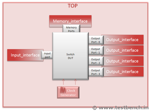
PHASE 1 TOP
In phase 1,
1) We will write SystemVerilog Interfaces for input port, output port and memory port.
2) We will write Top module where testcase and DUT instances are done.
3) DUT and TestBench interfaces are connected in top module.
4) Clock is generator in top module.
NOTE: In every file you will see the syntax
`ifndef GUARD_*
`endif GUARD_*
Interfaces
In the interface.sv file, declare the 3 interfaces in the following way.
 All the interfaces has clock as input.
All the signals in interface are logic type.
All the signals are synchronized to clock except reset in clocking block.
Signal directional w.r.t TestBench is specified with modport.
`ifndef GUARD_INTERFACE
`define GUARD_INTERFACE
//////////////////////////////////////////
// Interface declaration for the memory///
//////////////////////////////////////////
interface mem_interface(input bit clock);
logic [7:0] mem_data;
logic [1:0] mem_add;
logic mem_en;
logic mem_rd_wr;
clocking cb@(posedge clock);
default input #1 output #1;
output mem_data;
output mem_add;
output mem_en;
output mem_rd_wr;
endclocking
modport MEM(clocking cb,input clock);
endinterface
////////////////////////////////////////////
// Interface for the input side of switch.//
// Reset signal is also passed hear. //
////////////////////////////////////////////
interface input_interface(input bit clock);
logic data_status;
logic [7:0] data_in;
logic reset;
clocking cb@(posedge clock);
default input #1 output #1;
output data_status;
output data_in;
endclocking
modport IP(clocking cb,output reset,input clock);
endinterface
/////////////////////////////////////////////////
// Interface for the output side of the switch.//
// output_interface is for only one output port//
/////////////////////////////////////////////////
interface output_interface(input bit clock);
logic [7:0] data_out;
logic ready;
logic read;
clocking cb@(posedge clock);
default input #1 output #1;
input data_out;
input ready;
output read;
endclocking
modport OP(clocking cb,input clock);
endinterface
//////////////////////////////////////////////////
`endif
Testcase
Testcase is a program block which provides an entry point for the test and creates a scope that encapsulates program-wide data. Currently this is an empty testcase which just ends the simulation after 100 time units. Program block contains all the above declared interfaces as arguments. This testcase has initial and final blocks.
`ifndef GUARD_TESTCASE
`define GUARD_TESTCASE
program testcase(mem_interface.MEM mem_intf,input_interface.IP input_intf,output_interface.OP output_intf[4]);
initial
begin
$display(" ******************* Start of testcase ****************");
#1000;
end
final
$display(" ******************** End of testcase *****************");
endprogram
`endif
Top Module
The modules that are included in the source text but are not instantiated are called top modules. This module is the highest scope of modules. Generally this module is named as "top" and referenced as "top module". Module name can be anything.
Do the following in the top module:
1)Generate the clock signal.
bit Clock;
initial
forever #10 Clock = ~Clock;
2)Do the instances of memory interface.
mem_interface mem_intf(Clock);
3)Do the instances of input interface.
input_interface input_intf(Clock);
4)There are 4 output ports. So do 4 instances of output_interface.
output_interface output_intf[4](Clock);
5)Do the instance of testcase and pass all the above declared interfaces.
testcase TC (mem_intf,input_intf,output_intf);
6)Do the instance of DUT.
switch DUT (.
7)Connect all the interfaces and DUT. The design which we have taken is in verilog. So Verilog DUT instance is connected signal by signal.
switch DUT (.clk(Clock),
.reset(input_intf.reset),
.data_status(input_intf.data_status),
.data(input_intf.data_in),
.port0(output_intf[0].data_out),
.port1(output_intf[1].data_out),
.port2(output_intf[2].data_out),
.port3(output_intf[3].data_out),
.ready_0(output_intf[0].ready),
.ready_1(output_intf[1].ready),
.ready_2(output_intf[2].ready),
.ready_3(output_intf[3].ready),
.read_0(output_intf[0].read),
.read_1(output_intf[1].read),
.read_2(output_intf[2].read),
.read_3(output_intf[3].read),
.mem_en(mem_intf.mem_en),
.mem_rd_wr(mem_intf.mem_rd_wr),
.mem_add(mem_intf.mem_add),
.mem_data(mem_intf.mem_data));
Top Module Source Code:
`ifndef GUARD_TOP
`define GUARD_TOP
module top();
/////////////////////////////////////////////////////
// Clock Declaration and Generation //
/////////////////////////////////////////////////////
bit Clock;
initial
forever #10 Clock = ~Clock;
/////////////////////////////////////////////////////
// Memory interface instance //
/////////////////////////////////////////////////////
mem_interface mem_intf(Clock);
/////////////////////////////////////////////////////
// Input interface instance //
/////////////////////////////////////////////////////
input_interface input_intf(Clock);
/////////////////////////////////////////////////////
// output interface instance //
/////////////////////////////////////////////////////
output_interface output_intf[4](Clock);
/////////////////////////////////////////////////////
// Program block Testcase instance //
/////////////////////////////////////////////////////
testcase TC (mem_intf,input_intf,output_intf);
/////////////////////////////////////////////////////
// DUT instance and signal connection //
/////////////////////////////////////////////////////
switch DUT (.clk(Clock),
.reset(input_intf.reset),
.data_status(input_intf.data_status),
.data(input_intf.data_in),
.port0(output_intf[0].data_out),
.port1(output_intf[1].data_out),
.port2(output_intf[2].data_out),
.port3(output_intf[3].data_out),
.ready_0(output_intf[0].ready),
.ready_1(output_intf[1].ready),
.ready_2(output_intf[2].ready),
.ready_3(output_intf[3].ready),
.read_0(output_intf[0].read),
.read_1(output_intf[1].read),
.read_2(output_intf[2].read),
.read_3(output_intf[3].read),
.mem_en(mem_intf.mem_en),
.mem_rd_wr(mem_intf.mem_rd_wr),
.mem_add(mem_intf.mem_add),
.mem_data(mem_intf.mem_data));
endmodule
`endif
(S)Download the phase 1 files:
switch_1.tar
Browse the code in switch_1.tar
(S)Run the simulation:
vcs -sverilog -f filelist -R -ntb_opts dtm
(S)Log file after simulation:
******************* Start of testcase ****************
******************** End of testcase *****************
In phase 1,
1) We will write SystemVerilog Interfaces for input port, output port and memory port.
2) We will write Top module where testcase and DUT instances are done.
3) DUT and TestBench interfaces are connected in top module.
4) Clock is generator in top module.
NOTE: In every file you will see the syntax
`ifndef GUARD_*
`endif GUARD_*
Interfaces
In the interface.sv file, declare the 3 interfaces in the following way.
All the interfaces has clock as input.
All the signals in interface are logic type.
All the signals are synchronized to clock except reset in clocking block.
Signal directional w.r.t TestBench is specified with modport.
`ifndef GUARD_INTERFACE
`define GUARD_INTERFACE
//////////////////////////////////////////
// Interface declaration for the memory///
//////////////////////////////////////////
interface mem_interface(input bit clock);
logic [7:0] mem_data;
logic [1:0] mem_add;
logic mem_en;
logic mem_rd_wr;
clocking cb@(posedge clock);
default input #1 output #1;
output mem_data;
output mem_add;
output mem_en;
output mem_rd_wr;
endclocking
modport MEM(clocking cb,input clock);
endinterface
////////////////////////////////////////////
// Interface for the input side of switch.//
// Reset signal is also passed hear. //
////////////////////////////////////////////
interface input_interface(input bit clock);
logic data_status;
logic [7:0] data_in;
logic reset;
clocking cb@(posedge clock);
default input #1 output #1;
output data_status;
output data_in;
endclocking
modport IP(clocking cb,output reset,input clock);
endinterface
/////////////////////////////////////////////////
// Interface for the output side of the switch.//
// output_interface is for only one output port//
/////////////////////////////////////////////////
interface output_interface(input bit clock);
logic [7:0] data_out;
logic ready;
logic read;
clocking cb@(posedge clock);
default input #1 output #1;
input data_out;
input ready;
output read;
endclocking
modport OP(clocking cb,input clock);
endinterface
//////////////////////////////////////////////////
`endif
Testcase
Testcase is a program block which provides an entry point for the test and creates a scope that encapsulates program-wide data. Currently this is an empty testcase which just ends the simulation after 100 time units. Program block contains all the above declared interfaces as arguments. This testcase has initial and final blocks.
`ifndef GUARD_TESTCASE
`define GUARD_TESTCASE
program testcase(mem_interface.MEM mem_intf,input_interface.IP input_intf,output_interface.OP output_intf[4]);
initial
begin
$display(" ******************* Start of testcase ****************");
#1000;
end
final
$display(" ******************** End of testcase *****************");
endprogram
`endif
Top Module
The modules that are included in the source text but are not instantiated are called top modules. This module is the highest scope of modules. Generally this module is named as "top" and referenced as "top module". Module name can be anything.
Do the following in the top module:
1)Generate the clock signal.
bit Clock;
initial
forever #10 Clock = ~Clock;
2)Do the instances of memory interface.
mem_interface mem_intf(Clock);
3)Do the instances of input interface.
input_interface input_intf(Clock);
4)There are 4 output ports. So do 4 instances of output_interface.
output_interface output_intf[4](Clock);
5)Do the instance of testcase and pass all the above declared interfaces.
testcase TC (mem_intf,input_intf,output_intf);
6)Do the instance of DUT.
switch DUT (.
7)Connect all the interfaces and DUT. The design which we have taken is in verilog. So Verilog DUT instance is connected signal by signal.
switch DUT (.clk(Clock),
.reset(input_intf.reset),
.data_status(input_intf.data_status),
.data(input_intf.data_in),
.port0(output_intf[0].data_out),
.port1(output_intf[1].data_out),
.port2(output_intf[2].data_out),
.port3(output_intf[3].data_out),
.ready_0(output_intf[0].ready),
.ready_1(output_intf[1].ready),
.ready_2(output_intf[2].ready),
.ready_3(output_intf[3].ready),
.read_0(output_intf[0].read),
.read_1(output_intf[1].read),
.read_2(output_intf[2].read),
.read_3(output_intf[3].read),
.mem_en(mem_intf.mem_en),
.mem_rd_wr(mem_intf.mem_rd_wr),
.mem_add(mem_intf.mem_add),
.mem_data(mem_intf.mem_data));
Top Module Source Code:
`ifndef GUARD_TOP
`define GUARD_TOP
module top();
/////////////////////////////////////////////////////
// Clock Declaration and Generation //
/////////////////////////////////////////////////////
bit Clock;
initial
forever #10 Clock = ~Clock;
/////////////////////////////////////////////////////
// Memory interface instance //
/////////////////////////////////////////////////////
mem_interface mem_intf(Clock);
/////////////////////////////////////////////////////
// Input interface instance //
/////////////////////////////////////////////////////
input_interface input_intf(Clock);
/////////////////////////////////////////////////////
// output interface instance //
/////////////////////////////////////////////////////
output_interface output_intf[4](Clock);
/////////////////////////////////////////////////////
// Program block Testcase instance //
/////////////////////////////////////////////////////
testcase TC (mem_intf,input_intf,output_intf);
/////////////////////////////////////////////////////
// DUT instance and signal connection //
/////////////////////////////////////////////////////
switch DUT (.clk(Clock),
.reset(input_intf.reset),
.data_status(input_intf.data_status),
.data(input_intf.data_in),
.port0(output_intf[0].data_out),
.port1(output_intf[1].data_out),
.port2(output_intf[2].data_out),
.port3(output_intf[3].data_out),
.ready_0(output_intf[0].ready),
.ready_1(output_intf[1].ready),
.ready_2(output_intf[2].ready),
.ready_3(output_intf[3].ready),
.read_0(output_intf[0].read),
.read_1(output_intf[1].read),
.read_2(output_intf[2].read),
.read_3(output_intf[3].read),
.mem_en(mem_intf.mem_en),
.mem_rd_wr(mem_intf.mem_rd_wr),
.mem_add(mem_intf.mem_add),
.mem_data(mem_intf.mem_data));
endmodule
`endif
(S)Download the phase 1 files:
switch_1.tar
Browse the code in switch_1.tar
(S)Run the simulation:
vcs -sverilog -f filelist -R -ntb_opts dtm
(S)Log file after simulation:
******************* Start of testcase ****************
******************** End of testcase *****************
Index
Introduction
Specification
Verification Plan
Phase 1 Top
Phase 2 Environment
Phase 3 Reset
Phase 4 Packet
Phase 5 Driver
Phase 6 Receiver
Phase 7 Scoreboard
Phase 8 Coverage
Phase 9 Testcase
Report a Bug or Comment on This section - Your input is what keeps Testbench.in improving with time!

Introduction
Specification
Verification Plan
Phase 1 Top
Phase 2 Environment
Phase 3 Reset
Phase 4 Packet
Phase 5 Driver
Phase 6 Receiver
Phase 7 Scoreboard
Phase 8 Coverage
Phase 9 Testcase
Report a Bug or Comment on This section - Your input is what keeps Testbench.in improving with time!